Introduction
Even 15-20 years ago, many did not even think about the possible replacement of silicon. Few could have imagined that already at the beginning of the twenty-first century, a real “nanometer race” would begin between semiconductor companies. Gradual rapprochement with the nanoworld makes you wonder what will happen next? Will the famous Moore's law be continued? After all, with the transition to thinner production norms Developers face increasingly complex challenges. Many experts are generally inclined to believe that in a dozen or two years silicon will approach a physically insurmountable limit, when it will no longer be possible to create thinner silicon structures.
Judging by recent research, one of the most likely (but by no means the only) candidates for the position of "silicon substitutes" are carbon-based materials - carbon nanotubes and graphene - which, presumably, can become the basis of future nanoelectronics. We wanted to talk about them in this article. Rather, we will talk still more about nanotubes, since they were obtained earlier and are better studied. There are far fewer developments related to graphene, but this does not detract from its dignity. Some researchers believe that graphene is a more promising material than carbon nanotubes, so we will also say a few words about it today. Moreover, some recent achievements of researchers give a little optimism.
In fact, it is very difficult to cover all the achievements in these rapidly developing areas within the framework of one article, so we will focus only on the key events of recent months. The purpose of the article is to briefly acquaint readers with the most important and most interesting recent achievements in the field of "carbon" nanoelectronics and promising areas of its application. For those who are interested, finding a lot of more detailed information on this topic should not be difficult (especially with knowledge of English).
carbon nanotubes
After another one (fullerenes) was added to the traditional three allotropic forms of carbon (graphite, diamond and carbine), over the next few years, reports were pouring in from research laboratories about the discovery and study of various carbon-based structures with interesting properties, such as nanotubes, nanorings, ultrafine materials, etc.
First of all, we are interested in carbon nanotubes - hollow elongated cylindrical structures with a diameter of a few to tens of nanometers (the length of traditional nanotubes is calculated in microns, although structures with a length of the order of millimeters and even centimeters are already being obtained in laboratories). These nanostructures can be represented as follows: we simply take a strip of a graphite plane and roll it into a cylinder. Of course, this is just a figurative representation. In reality, it is not possible to directly obtain a graphite plane and twist it “into a tube”. Methods for obtaining carbon nanotubes are a rather complex and voluminous technical problem, and their consideration is beyond the scope of this article.
 |
Carbon nanotubes are characterized by a wide variety of shapes. For example, they can be single-walled or multi-walled (single-layer or multi-layered), straight or helical, long or short, etc. Importantly, nanotubes have proven to be remarkably strong in tension and bending. Under the action of high mechanical stresses, nanotubes do not tear or break, but their structure is simply rearranged. By the way, since we are talking about the strength of nanotubes, it is interesting to note one of the latest studies on the nature of this property.
Rice University researchers led by Boris Jacobson have found that carbon nanotubes behave like "smart self-healing structures" (the study was published February 16, 2007 in the journal Physical Review Letters). So, with a critical mechanical impact and deformations caused by changes in temperature or radioactive radiation, nanotubes can "repair" themselves. It turns out that in addition to 6-carbon cells, nanotubes also contain five- and seven-atom clusters. These 5/7-atom cells exhibit unusual behavior, cycling along the surface of the carbon nanotube like steamboats on the sea. When damage occurs at the site of the defect, these cells take part in the "wound healing", redistributing energy.
In addition, nanotubes exhibit many unexpected electrical, magnetic, and optical properties, which have already become the objects of a number of studies. A feature of carbon nanotubes is their electrical conductivity, which turned out to be higher than that of all known conductors. They also have excellent thermal conductivity, are chemically stable and, most interestingly, can acquire semiconducting properties. In terms of electronic properties, carbon nanotubes can behave like metals or like semiconductors, which is determined by the orientation of the carbon polygons relative to the tube axis.
Nanotubes tend to adhere tightly to each other, forming sets consisting of metal and semiconductor nanotubes. Until now, a difficult task is the synthesis of an array of only semiconductor nanotubes or the separation (separation) of semiconductor nanotubes from metal ones. We will get acquainted with the latest methods of solving this problem further.
Graphene
Graphene, compared to carbon nanotubes, was obtained much later. Perhaps this explains the fact that so far we hear about graphene in the news much less often than about carbon nanotubes, since it is less studied. But this does not detract from its merits. By the way, a couple of weeks ago, graphene was in the spotlight in scientific circles, thanks to a new development by researchers. But more on that later, but now a little history.
In October 2004, the BBC News information resource reported that Professor Andre Geim and his colleagues from the University of Manchester (UK), together with the group of Dr. Novoselov (Chernogolovka, Russia), managed to obtain a material one carbon atom thick. Called graphene, it is a two-dimensional planar carbon molecule one atom thick. For the first time in the world, it was possible to separate an atomic layer from a graphite crystal.

At the same time, Game and his team proposed the so-called graphene-based ballistic transistor. Graphene will make it possible to create transistors and other semiconductor devices with very small dimensions (of the order of several nanometers). Reducing the length of the transistor channel leads to a change in its properties. In the nanoworld, the role of quantum effects is increasing. Electrons move through the channel like a de Broglie wave, and this reduces the number of collisions and, accordingly, increases the energy efficiency of the transistor.
Graphene can be thought of as an "unfolded" carbon nanotube. The increased mobility of electrons makes it one of the most promising materials for nanoelectronics. Since less than three years have passed since the receipt of graphene, its properties have not yet been studied very well. But the first interesting results of the experiments are already there.

Latest carbon advances
Since we first got acquainted with carbon nanotubes (chronologically, they were the first to be obtained), in this part of the article we will also start with them. Probably, you may have the following question: if carbon nanotubes are so good and promising, why haven't they been introduced into mass production yet?
One of the main problems was already mentioned at the beginning of the article. A method for synthesizing an array consisting only of nanotubes with certain properties, shape and dimensions, which could be introduced into mass production, has not yet been created. More attention is paid to the sorting of a "mixed" array consisting of nanotubes with semiconductor and metallic properties (sorting by length and diameter is no less important). Here it is appropriate to recall one of the first developments in this area, which belongs to IBM, after which we will move on to the latest achievements.
An April 2001 paper, "Engineering Carbon Nanotubes and Nanotube Circuits Using Electrical Breakdown," reports that IBM researchers have for the first time built a transistor based on carbon nanotubes 1 nanometer in diameter and a few microns long. Attention was focused on the fact that they managed to find a way to make such production mass in the future.
Scientists at IBM developed a method that allowed them to destroy all metal nanotubes while leaving semiconductor ones intact. In the first step, an array of nanotubes is placed on a silicon dioxide substrate. Next, electrodes are formed on top of the nanotubes. The silicon substrate plays the role of the bottom electrode and facilitates the blocking of semiconductor nanotubes. Then the overvoltage is applied. As a result, "unprotected" nanotubes with metallic properties are destroyed, while semiconductor ones remain intact.

But this is all just in words, but in reality the process itself looks much more complicated. Plans were reported to bring the development to perfection in 3-4 years (i.e., by 2004/2005), but, as we can see, there have been no reports of the introduction of this technology yet.
Now let's move on to the present, namely, the end of last autumn. Then the Technology Review website reported on a new method for sorting carbon nanotubes, which was developed by researchers at Northwestern University (Northwestern University). In addition to separation based on conductive properties, this method also allows nanotubes to be sorted by their diameter.
It is curious that initially the goal was to sort only by diameter, and the possibility of sorting by electrical conductivity was a surprise to the researchers themselves. Professor of Chemistry at the University of Montreal (Montreal, Canada) Richard Martel noted that the new sorting method can be called a major breakthrough in this area.
The new sorting method is based on ultracentrifugation, which involves the rotation of the material at high speeds up to 64 thousand revolutions per minute. Before that, a surfactant is applied to the array of nanotubes, which, after ultracentrifugation, is distributed unevenly in accordance with the diameter and electrical conductivity of the nanotubes. One of those who closely familiarized with the new method, University of Florida (University of Florida at Gainesville) professor Andrew Rinzler said that the proposed sorting method will allow to obtain an array with a concentration of semiconductor tubes of 99% and higher.
The new technology has already been used for experimental purposes. Using sorted semiconductor nanotubes, transistors with a relatively simple structure have been created that can be used to control pixels in monitor and TV panels.
By the way, unlike the IBM method, when metal nanotubes were simply destroyed, researchers at Northwestern University can also obtain metal nanotubes using ultracentrifugation, which can also be used in electronic devices. For example, they can be used as transparent electrodes in some types of displays and organic solar cells.
We will not delve into other problems that prevent the introduction of nanotubes, such as technological difficulties in integrating into serial electronic devices, as well as significant energy losses at the junctions of metal with nanotubes, which is due to the high contact resistance. Most likely, the disclosure of these serious topics will seem of little interest and too complicated for the average reader, moreover, it may take several pages.
As for graphene, let's start reviewing achievements in this area in the spring of last year. In April 2006, the journal Science Express published a fundamental study of the properties of graphene, conducted by a group of scientists from Technological Institute Georgia (Georgia Institute of Technology (GIT), USA) and the National Center scientific research France (Centre National de la Recherche Scientifique).
The first important thesis of the work is that graphene-based electronic circuits can be produced by traditional equipment used in the semiconductor industry. GIT Institute professor Walt de Heer summarized the success of the study as follows: “We have shown that we can create a graph new material, "cut" graphene structures, and that graphene has excellent electrical properties. This material is characterized by high electron mobility.”
Many scientists and researchers themselves say that they laid the foundation (base) of graphene electronics. It is noted that carbon nanotubes are only the first step towards the world of nanoelectronics. In the future of electronics, Walt de Heer and his colleagues see exactly graphene. It is noteworthy that the research is supported by Intel, and it does not throw money down the drain.
Let us now briefly describe the method for obtaining graphene and graphene microcircuits proposed by Walt de Heer and his colleagues. By heating a silicon carbide substrate in a high vacuum, the scientists force the silicon atoms to leave the substrate, leaving only a thin layer of carbon atoms (graphene). In the next step, they apply a photoresist material (photoresist) and use traditional electron beam lithography to etch the desired "patterns", that is, they use commonly used manufacturing technologies today. This is a significant advantage of graphene over nanotubes.

As a result, scientists were able to etch 80-nm nanostructures. In this way, a graphene field-effect transistor was created. A serious drawback can be called the large leakage currents of the created device, although scientists at that time were not upset at all. They believed that at the initial stage this is quite normal. In addition, a fully functional quantum interference device has been created that can be used to control electronic waves.

Since the spring of last year, there have been no high-profile achievements like the April development. At least they did not appear on the pages of Internet sites. But February of this year was marked by several events at once and again made me think about “graphene prospects”.
At the beginning of last month, AMO (AMO nanoelectronics group) presented its development as part of the ALEGRA project. AMO engineers have managed to create a graphene top-gated transistor, which makes their structure similar to modern silicon field-effect transistors (MOSFETs). Interestingly, the graphene transistor was created using traditional CMOS manufacturing technology.

Unlike MOSFETs (MOS - Metal Oxide Semiconductor), graphene transistors created by AMO engineers are characterized by higher electron mobility and switching speed. Unfortunately, at the moment the details of the development are not disclosed. The first details will be published in April this year in the IEEE Electron Device Letters.
Now let's move on to another "fresh" development - a graphene transistor that works as a single-electron semiconductor device. Interestingly, the creators of this device are already known to us Professor Geim, Russian scientist Konstantin Novoselov and others.

This transistor has regions in which electric charge becomes quantized. In this case, the effect of the Coulomb blockade is observed (during the transition of the electron, a voltage appears that prevents the movement of the following particles, it repels its fellows with its charge. This phenomenon was called the Coulomb blockade. Due to the blockade, the next electron will pass only when the previous one moves away from the transition. Thus, the particles can "jump" only at certain intervals of time). As a result, only one electron can pass through the channel of the transistor, which is only a few nanometers wide. That is, it becomes possible to control semiconductor devices with just one electron.
The ability to control individual electrons opens up new opportunities for the creators of electronic circuits. As a result, the gate voltage can be significantly reduced. Devices based on single-electron graphene transistors will be characterized by high sensitivity and excellent speed performance. Of course, the dimensions will also decrease by an order of magnitude. What matters is overcome serious problem, characteristic of the prototype graphene transistor Walt de Heer, - large leakage currents.
It should be noted that single-electron devices have already been created using traditional silicon. But the problem is that most of them can only work at very low temperatures (although there are already samples that work at room temperature, but they are much larger than graphene transistors). The brainchild of Geim and his colleagues can easily work at room temperature.
Prospects for the use of carbon nanomaterials
Most likely, this part of the article will be the most interesting to readers. After all, theory is one thing, and the embodiment of the achievements of science in real useful to man devices, even prototypes, should be of interest to the consumer. Generally speaking, the possible scope of application of carbon nanotubes and graphene is quite diverse, but we are primarily interested in the world of electronics. I would like to note right away that graphene is a “younger” carbon material and is still only at the beginning of the research path, therefore, in this part of the article, the focus will be on devices and technologies based on carbon nanotubes.
Displays
The use of carbon nanotubes in displays is closely related to the FED (Field Emission Display) technology, which was developed by the French company LETI and was first introduced back in 1991. Unlike a CRT, which uses up to three so-called "hot" cathodes, FED displays initially used a matrix of many "cold" cathodes. As it turned out, too high a reject rate made FED displays uncompetitive. In addition, in 1997-1998 there was a trend towards a significant reduction in the cost of liquid crystal panels, which, as it seemed then, left no chance for FED technology.
The brainchild of LETI received a "second wind" by the end of the last century, when the first studies of FED displays appeared, in which it was proposed to use arrays of carbon nanotubes as cathodes. A number of major manufacturers have shown interest in carbon nanotube displays, including Samsung, Motorola, Fujitsu, Canon, Toshiba, Philips, LG, Hitachi, Pioneer and others, well-known to everyone. In the illustration you see one of the options for implementing FED displays on carbon nanotubes SDNT (small diameter carbon nanotubes, carbon nanotubes of small diameter).

It is noted that FED-displays on carbon nanotubes can compete with modern panels with a large diagonal and in the future will seriously compete primarily with plasma panels (they now dominate the sector with super-large diagonals). Most importantly, carbon nanotubes will significantly reduce the cost of manufacturing FED displays.
From the latest news in the world of nanotube FED displays, it is worth recalling the recent announcement by Motorola that its developments are almost ready to leave the walls of research laboratories and move into mass production. Interestingly, Motorola does not plan to build its own factories for the production of nanotube displays and is currently in licensing negotiations with several manufacturers. Motorola's head of research and development, James Jaskie, noted that two Asian companies are already building factories to produce carbon nanotube displays. So nanotube displays are not so distant future, and it is time to take them seriously.
One of difficult tasks that presented themselves to the Motorola engineers was the creation of a low-temperature method for obtaining carbon nanotubes on a substrate (so as not to melt the glass substrate). And this technological barrier has already been overcome. It also reports the successful completion of the development of methods for sorting nanotubes, which for many companies operating in this industry has become an "insurmountable obstacle."
Director of DiplaySearch Steve Jurichich (Steve Jurichich) believes that it is too early to rejoice at Motorola. After all, there is still a conquest of the market ahead, where the place "under the sun" has already been taken by manufacturers of liquid crystal and plasma panels. Do not forget about other promising technologies, such as OLED (organic light-emitting diode displays), QD-LED (quantum-dot LED, a kind of LED displays using the so-called quantum dots, developed by the American company QD Vision). In addition, Samsung Electronics and a joint project on the introduction of Canon and Toshiba nanotube displays (by the way, they plan to start deliveries of the first nanotube displays by the end of this year).
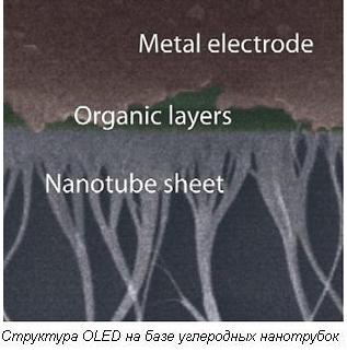
Carbon nanotubes have found application not only in FED displays. Researchers at the Regroupement Quebecois sur les Materiaux de Pointe laboratory (Quebec, Canada) proposed using a material based on single-walled carbon nanotubes as electrodes for OLED displays. According to the Nano Technology World website, the new technology will allow the creation of very thin electronic paper. Due to the high strength of the nanotubes and the extremely thin electrode array, OLED displays can be very flexible and also have a high degree of transparency.
 |
 |
Memory
Before starting a story about the most interesting "carbon" developments in the field of memory, I would like to note that research on information storage technologies in general is one of the most actively developing areas at the present time. The recent Consumer Electronic Show (Las Vegas) and Hanover CeBIT showed that interest in various drives and data storage systems does not subside over time, but only increases. And this is not surprising. Just think: according to analytical organization IDC, in 2006, about 161 billion gigabytes of information (161 exabytes) were generated, which is ten times more than in previous years!
During the past 2006, one could only marvel at the inventive ideas of scientists. What have we just not seen: memory on gold nanoparticles, and memory based on superconductors, and even memory ... on viruses and bacteria! Recently, more and more often in the news such non-volatile memory technologies as MRAM, FRAM, PRAM and others are mentioned, which are no longer only “paper” exhibits or demonstration prototypes, but quite efficient devices. So carbon nanotube-based memory technologies are only a small part of the research on information storage.
Perhaps, we will begin our story about "nanotube" memory with the developments of Nantero, which has already become quite famous in its field. It all started back in 2001, when large investments were attracted to the young company, which made it possible to start active development of a new type of non-volatile NRAM memory based on carbon nanotubes. Last year we saw some serious developments by Nantero. In April 2006, the company announced the creation of an NRAM-type memory switch manufactured to the 22nm standard. In addition to proprietary Nantero developments, existing manufacturing technologies were involved in the creation of a new device. In May of the same year, its carbon nanotube device technology was successfully integrated into CMOS manufacturing at LSI Logic Corporation (at ON Semiconductor's factory).
At the end of 2006, a significant event took place. Nantero announced that it has overcome all major technological barriers to mass production of carbon nanotube chips using traditional equipment. A method has been developed for depositing nanotubes on a silicon substrate using such a well-known method as spin-coating, after which lithography and etching, traditional for semiconductor production, are used. One of the advantages of NRAM-memory is high read / write speeds.

However, we will not delve into the technical subtleties. I will only note that such achievements give Nantero every reason to count on success. If the company's engineers manage to bring the development to its logical conclusion and the production of NRAM chips will not be very expensive (and the possibility of using existing equipment gives the right to hope for this), then we will witness the emergence of a new formidable weapon in the memory market, which can seriously oust existing types of memory, including SRAM, DRAM, NAND, NOR, etc.
As in many other areas of science and technology, carbon nanotube memory research is carried out not only by commercial companies such as Nantero, but also by laboratories of the world's leading educational institutions. Among the interesting works devoted to "carbon" memory, I would like to note the development of employees of the Hong Kong polytechnic university(Hong-Kong Polytechnic University), published in April last year on the pages of the online edition of Applied Physics Letters.
Unlike many similar developments that function only at very low temperatures, the device created by physicists Jiyan Dai and Lu (X. B. Lu) can work at room temperature. The non-volatile memory created by Hong Kong researchers is not as fast as Nantero's NRAM, so the prospect of removing DRAM from the throne is likely to fail. But as a potential replacement for traditional flash memory, it can be considered.
In order to understand in in general terms how this memory works, just look at illustration (b) below. Carbon nanotubes (CNT, carbon nanotubes) play the role of a charge storage (memory) layer. They seem to be sandwiched between two layers of HfAlO (consisting of hafnium, aluminum and oxygen), which play the role of a control gate and an oxide layer. The entire structure is placed on a silicon substrate.

A rather original solution was proposed by Korean scientists Jon Won Kang (Jeong Won Kang) and Kin Yan (Qing Jiang). They managed to develop a memory based on the so-called telescopic nanotubes. The underlying principle new development, was discovered back in 2002 and was described in the work "Multiwalled Carbon Nanotubes as Gigahertz Oscillators". Its authors managed to establish that a nanotube with another nanotube of smaller diameter embedded in it forms an oscillator, reaching a frequency of oscillations of the order of gigahertz.
The high sliding speed of nanotubes nested in other nanotubes determines the speed of a new type of memory. Yong Won Kang and Kin Yan argue that their design can be used not only as flash memory, but also as high-speed RAM. The principle of memory operation is easy to understand based on the figure.

As you can see, a pair of nested nanotubes is placed between two electrodes. When a charge is applied to one of the electrodes, the inner nanotube moves in one direction or another under the action of van der Waals forces. This development has one significant drawback: a sample of such memory can only work at very low temperatures. However, scientists are confident that these problems are temporary and can be overcome in the next stages of research.
Quite naturally, many developments will remain stillborn. After all, a prototype working in the laboratory is one thing, but on the way to the commercialization of technology there are always many difficulties, and not only purely technical, but also material ones. In any case, the existing works inspire a certain optimism and are quite informative.
Processors
Now let's dream about what kind of carbon future processors can have. The giants of the processor industry are actively looking for new ways to extend Gordon Moore's law, and every year it becomes more and more difficult for them. The reduction in the size of semiconductor elements and the huge density of their placement on a crystal each time poses a very difficult task of reducing leakage currents. The main directions for solving such problems are the search for new materials for use in semiconductor devices and changing their very structure.
As you probably know, recently IBM and Intel almost simultaneously announced the use of new materials to create transistors that will be used in the next generation of processors. Hafnium-based materials with a high dielectric constant (high-k) have been proposed as a gate dielectric instead of silicon dioxide. When creating a gate electrode, silicon will be displaced by metal alloys.

As we can see, even today there is a gradual replacement of silicon and materials based on it with more promising compounds. Many companies have been thinking about replacing silicon for a long time. One of the biggest sponsors research projects in the field of carbon nanotubes and graphene are IBM and Intel.
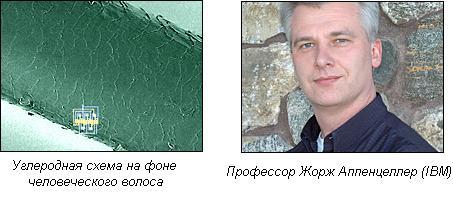
At the end of March last year, a group of researchers from IBM and two universities in Florida and New York announced the creation of the first complete electronic integrated circuit based on just one carbon nanotube. This scheme is five times thinner than the diameter of a human hair and can only be observed through a powerful electron microscope.
IBM researchers have been able to achieve speeds nearly a million times faster than previously achieved with multiple nanotube circuits. Although these speeds are still slower than today's silicon chips, IBM scientists are confident that new nanotechnology processes will eventually unlock the enormous potential of carbon nanotube electronics.
According to Professor Joerg Appenzeller, the nanotube-based ring oscillator created by the researchers is an excellent tool for studying the characteristics of carbon electronic elements. A ring oscillator is a circuit in which chip manufacturers typically test the feasibility of new manufacturing processes or materials. This schema helps predict how new technologies will behave in finished products.
For a relatively long time, Intel has been conducting its research on the possible use of carbon nanotubes in processors. Recall that Intel is not indifferent to nanotubes, forced the recent event Symposium for the American Vacuum Society, which actively discussed the latest achievements of the company in this area.
By the way, a prototype chip has already been developed, where carbon nanotubes are used as interconnects. As is known. the transition to more precise standards entails an increase in the electrical resistance of the connecting conductors In the late 90s, microcircuit manufacturers switched to using copper conductors instead of aluminum ones. But already in recent years, even copper has ceased to satisfy processor manufacturers, and gradually they are preparing a replacement for it.
One of the promising directions is the use of carbon nanotubes. By the way, as we mentioned at the beginning of the article, carbon nanotubes not only have better conductivity compared to metals, but can also play the role of semiconductors. Thus, there seems to be a real possibility in the future to completely replace silicon in processors and other microcircuits and create chips made entirely of carbon nanotubes.
On the other hand, it is also too early to “bury” silicon. First, the complete displacement of silicon by carbon nanotubes in microcircuits is unlikely to occur in the next decade. And this is noted by the authors of successful developments themselves. Secondly, silicon also has prospects. In addition to carbon nanotubes, silicon also has a chance to secure a future in nanoelectronics - in the form of silicon nanowires, nanotubes, nanodots and other structures, which are also the subject of study in many research laboratories.
Afterword
In conclusion, I would like to add that this article managed to cover only a very small part of what is currently happening in the field of carbon nanoelectronics. Bright minds continue to invent sophisticated technologies, some of which may become the foundation of the electronics of the future. Some tend to believe that nanorobots, transparent displays, televisions that can be twisted into a thin tube, and other amazing devices remain fiction and will become reality only in the very distant future. But a number of amazing studies already today make us think that all this is not such a distant prospect.
In addition, apart from the carbon nanotubes and graphene discussed in this article, amazing discoveries are taking place in molecular electronics. Curious research is being carried out in the field of communication between the biological and silicon worlds. There are many prospects for the development of the computer industry. And no one will probably undertake to predict what will happen in 10-15 years. One thing is clear: there are still many exciting discoveries and amazing devices ahead of us.

Sources of information used when writing the article
- [email protected] ()
- PhysOrg.com ()))
- IBM Research()
- K. S. Novoselov, A. K. Geim, S. V. Morozov, D. Jiang, Y. Zhang, S. V. Dubonos, I. V. Grigorieva, A. A. Firsov. "Electric Field Effect in Atomically Thin Carbon Films"
- K. S. Novoselov, D. Jiang, F. Schedin, V. V. Khotkevich, S. V. Morozov, and A.K. Geim "Two-dimensional atomic crystals"
- Quanshui Zheng, Qing Jiang. "Multiwalled Carbon Nanotubes as Gigahertz Oscillators"
It is believed that the discoverer of carbon nanotubes is an employee of the Japanese corporation NEC Sumio Iijima, who in 1991 observed the structures of multilayer nanotubes when studying deposits under an electron microscope, which were formed during the synthesis of molecular forms of pure carbon having a cellular structure.
Classification
The main classification of nanotubes is based on the number of their constituent layers.
Single-walled nanotubes(single-walled nanotubes, SNWTs) - the simplest type of nanotubes. Most of them have a diameter of about 1 nm with a length that can be many thousands of times longer. The structure of single-walled nanotubes can be represented as a “wrapping” of a hexagonal network of graphite (graphene), which is based on hexagons with carbon atoms located at the corner vertices, into a seamless cylinder. The upper ends of the tubes are closed with hemispherical caps, each layer of which is composed of hexagons and pentagons, resembling the structure of half a fullerene molecule.
Figure 1. Graphical representation of a single-layer nanotube
Multilayer nanotubes(multi-walled nanotubes, MWNTs) consist of several layers of graphene stacked in the shape of a tube. The distance between the layers is 0.34 nm, i.e. the same as between the layers in crystalline graphite.
There are two models used to describe their structure. Multilayer nanotubes can be several single-layer nanotubes nested one inside the other (the so-called "matryoshka"). In another case, one "sheet" of graphene wraps around itself several times, which is similar to the scrolling of parchment or newspaper (the "parchment" model).

Figure 2. Graphic image of a multilayer nanotube (matryoshka model)
Synthesis methods
The most common methods for the synthesis of nanotubes are the electric arc method, laser ablation, and chemical vapor deposition (CVD).
Arc discharge - the essence of this method lies in the production of carbon nanotubes in an arc discharge plasma burning in a helium atmosphere at technological installations for the production of fullerenes. However, other modes of arcing are used here: low current densities of the arc discharge, higher helium pressure (~ 500 Torr), larger diameter cathodes.
To increase the yield of nanotubes in sputtering products, a catalyst (mixtures of iron group metals) is introduced into the graphite rod, the pressure of the inert gas and the sputtering mode are changed.
The content of nanotubes in the cathode deposit reaches 60%. The resulting nanotubes up to 40 μm in length grow from the cathode perpendicular to its surface and combine into cylindrical beams about 50 km in diameter.
Laser ablation
This method was invented by Richard Smalley and Rice University and is based on the evaporation of a graphite target in a high temperature reactor. Nanotubes appear on the cooled surface of the reactor as graphite evaporation condensate. The water-cooled surface can be included in the nanotube collection system.
The product yield in this method is about 70%. With its help, predominantly single-walled carbon nanotubes with a diameter controlled by the reaction temperature are obtained. However, the cost of this method is much more expensive than the others.
Chemical vapor deposition (CVD)
The method of catalytic carbon vapor deposition was discovered back in 1959, but until 1993 no one assumed that nanotubes could be obtained in this process.
In the process of this method, a substrate is prepared with a catalyst layer - metal particles (most often nickel, cobalt, iron, or combinations thereof). The diameter of nanotubes grown in this way depends on the size of the metal particles.
The substrate is heated to approximately 700°C. To initiate the growth of nanotubes, two types of gases are introduced into the reactor: process gas (for example, ammonia, nitrogen, hydrogen, etc.) and carbon-containing gas (acytylene, ethylene, ethanol, methane, etc.). Nanotubes begin to grow on the sites of metal catalysts.
This mechanism is the most common commercial method for the production of carbon nanotubes. Among other methods for obtaining nanotubes, CVD is the most promising on an industrial scale due to the best ratio in terms of unit price. In addition, it makes it possible to obtain vertically oriented nanotubes on the desired substrate without additional collection, as well as to control their growth by means of a catalyst.
Areas of use
Carbon nanotubes, together with fullerenes and mesoporous carbon structures, form a new class of carbon nanomaterials, or carbon framework structures, with properties that differ significantly from other forms of carbon such as graphite and diamond. However, nanotubes are the most promising among them.
Interested in nanomaterials business? Then you might be interested
The third state of carbon (except diamond and graphite) is revolutionizing the world of new technologies.Here are excerpts from several articles (with links to them).
http://www.nsu.ru/materials/ssl/text/news/Physics/135.html
Many of the promising areas in materials science, nanotechnology, nanoelectronics, and applied chemistry are associated with Lately with fullerenes, nanotubes and other similar structures, which can be called by the general term carbon framework structures. What is it?
Carbon frame structures are large (and sometimes gigantic!) molecules consisting exclusively of carbon atoms. One can even say that carbon framework structures are a new allotropic form of carbon (in addition to the long-known ones: diamond and graphite). main feature of these molecules - this is their skeletal form: they look like closed, empty inside the "shell".
Finally, the variety of applications that have already been devised for nanotubes is striking. The first thing that suggests itself is the use of nanotubes as very strong microscopic rods and threads. As the results of experiments and numerical simulations show, the Young's modulus of a single-layer nanotube reaches values of the order of 1-5 TPa, which is an order of magnitude greater than that of steel! True, at present, the maximum length of nanotubes is tens and hundreds of microns - which, of course, is very large on an atomic scale, but too small for everyday use. However, the length of nanotubes obtained in the laboratory is gradually increasing - now scientists have already come close to the millimeter limit: see the work, which describes the synthesis of a multilayer nanotube 2 mm long. Therefore, there is every reason to hope that in the near future, scientists will learn how to grow nanotubes that are centimeters and even meters long! Of course, this will greatly affect future technologies: after all, a “cable” as thick as a human hair, capable of holding a load of hundreds of kilograms, will find countless applications.
The unusual electrical properties of nanotubes will make them one of the main materials of nanoelectronics. Prototypes have already been created field effect transistors based on a single nanotube: by applying a blocking voltage of several volts, scientists have learned to change the conductivity of single-walled nanotubes by 5 orders of magnitude!
Several applications of nanotubes in the computer industry have already been developed. For example, prototypes of thin flat displays based on a nanotube matrix have been created and tested. Under the action of a voltage applied to one end of the nanotube, electrons begin to be emitted from the other end, which fall on the phosphorescent screen and cause the pixel to glow. The resulting image grain will be fantastically small: on the order of a micron!
http://brd.dorms.spbu.ru/nanotech/print.php?sid=44
An attempt to photograph nanotubes using a conventional camera with a flash led to the fact that the block of nanotubes emitted a loud pop in the light of the flash and, flashing brightly, exploded.
The dumbfounded scientists claim that the unexpectedly discovered phenomenon of "explosiveness" of tubes can find new, completely unexpected uses for this material - up to and including use as detonators to undermine warheads. And also, obviously, it will call into question or make it difficult to use them in certain areas.
http://www.sciteclibrary.com/rus/catalog/pages/2654.html
Opens the prospect of significantly extending the life of rechargeable batteries
http://vivovoco.nns.ru/VV/JOURNAL/VRAN/SESSION/NANO1.HTM
Carbon nanotube structures - a new material for emission electronics.
http://www.gazetangn.narod.ru/archive/ngn0221/space.html
Back in 1996, it was discovered that individual carbon nanotubes can spontaneously twist into cords of 100-500 fiber-tubules, and the strength of these cords turned out to be greater than that of diamond. More precisely, they are 10-12 times stronger and 6 times lighter than steel. Just imagine: a thread with a diameter of 1 millimeter could withstand a 20-ton load, hundreds of billions of times greater than its own weight! It is from such threads that you can get heavy-duty cables of great length. From equally light and durable materials, it is possible to build an elevator frame - a giant tower three times the diameter of the Earth. Passenger and cargo cabins will go along it at tremendous speed - thanks to superconducting magnets, which, again, will be suspended on carbon nanotube ropes. The colossal cargo flow into space will allow the active exploration of other planets to begin.
If someone is interested in this project, details (in Russian) can be found, for example, on the site http://private.peterlink.ru/geogod/space/future.htm. Only there is not a word about carbon tubes.
And on http://www.eunet.lv/library/win/KLARK/fontany.txt you can read Arthur Clarke's novel "Fountains of Paradise", which he himself considered his best work.
http://www.inauka.ru/science/28-08-01/article4805
According to experts, nanotechnology will make it possible by 2007 to create microprocessors that will contain about 1 billion transistors and will be able to operate at a frequency of up to 20 gigahertz with a supply voltage of less than 1 volt.
nanotube transistor
Created the first transistor, consisting entirely of carbon nanotubes. This opens up the prospect of replacing conventional silicon chips with faster, cheaper, and smaller components.
The world's first nanotube transistor is a Y-shaped nanotube that behaves like a familiar transistor - a potential applied to one of the "legs" allows you to control the passage of current between the other two. At the same time, the current-voltage characteristic of the “nanotube transistor” is almost ideal: current either flows or not.
http://www.pool.kiev.ua/clients/poolhome.nsf/0/a95ad844a57c1236c2256bc6003dfba8?OpenDocument
According to an article published on May 20 in scientific journal Applied Physics Letters, IBM specialists improved carbon nanotube transistors. As a result of experiments with various molecular structures, the researchers were able to achieve the highest conductivity to date for carbon nanotube transistors. The higher the conductivity, the faster the transistor works and the more powerful integrated circuits can be built based on it. In addition, the researchers found that the conductivity of carbon nanotube transistors is more than double that of the fastest silicon transistors of the same size.
http://kv.by/index2003323401.htm
A group of professor at the University of California at Berkeley Alex Zettl (Alex Zettl) made another breakthrough in the field of nanotechnology. Scientists have created the first smallest nanoscale motor based on multi-walled nanotubes, as reported in Nature on July 24. The carbon nanotube acts as a kind of axis on which the rotor is mounted. The maximum dimensions of a nanomotor are about 500 nm, the rotor has a length of 100 to 300 nm, but the nanotube-axis has a diameter of only a few atoms, i.e. about 5-10 nm.
http://www.computerra.ru/hitech/tech/26393/
The Boston-based company Nantero has recently announced the development of a fundamentally new type of memory cards based on nanotechnology. Nantero Inc. actively engaged in the development of new technologies, in particular, pays considerable attention to finding ways to create non-volatile random access memory (RAM) based on carbon nanotubes. In his speech, a company representative announced that they are one step away from creating 10 GB memory boards. Due to the fact that the structure of the device is based on nanotubes, it is proposed to call the new memory NRAM (Nonvolatile (non-volatile) RAM).
http://www.ixs.nm.ru/nan0.htm
One of the results of the study was the practical use of the outstanding properties of nanotubes to measure the mass of extremely small particles. When a particle to be weighed is placed at the end of the nanotube, the resonant frequency decreases. If the nanotube is calibrated (i.e., its elasticity is known), it is possible to determine the mass of the particle from the shift of the resonant frequency.
http://www.mediacenter.ru/a74.phtml
Among the first commercial applications will be the addition of nanotubes to paints or plastics to make these materials electrically conductive. This will allow replacing metal parts with polymer ones in some products.
Carbon nanotubes are an expensive material. Now CNI sells it for $500 per gram. In addition, the technology for cleaning carbon nanotubes - separating good tubes from bad ones - and the method of introducing nanotubes into other products need to be improved. Some challenges may require a Nobel-level discovery, says Joshua Wolf, managing partner at nanotechnology venture firm Lux Capital.
Researchers became interested in carbon nanotubes because of their electrical conductivity, which turned out to be higher than that of all known conductors. They also have excellent thermal conductivity, chemical stability, extreme mechanical strength (up to 1,000 times stronger than steel) and, most surprisingly, semiconducting properties when twisted or bent. To work, they are given the shape of a ring. The electronic properties of carbon nanotubes can be similar to those of metals or semiconductors (depending on the orientation of the carbon polygons relative to the axis of the tube), i.e. depend on their size and shape.
http://www.ci.ru/inform09_01/p04predel.htm
Metallic conductive nanotubes can withstand current densities 102-103 times higher than conventional metals, and semiconductor nanotubes can be electrically turned on and off by means of a field generated by an electrode, making it possible to create field-effect transistors.
Scientists at IBM have developed a method called "constructive destruction" that has allowed them to destroy all metal nanotubes while leaving the semiconductor ones intact.
http://www.pr.kg/articles/n0111/19-sci.htm
Carbon nanotubes have found another use in the fight for human health - this time, Chinese scientists have used nanotubes to purify drinking water from lead.
http://www.scientific.ru/journal/news/n030102.html
We regularly write about carbon nanotubes, but in fact there are other types of nanotubes made from various semiconductor materials. Scientists are able to grow nanotubes with precisely specified wall thickness, diameter and length.
Nanotubes can be used as nanopipes for transporting liquids, they can also act as syringe tips with a precisely calibrated amount of nanodroplets. Nanotubes can be used as nanodrills, nanotweezers, tips for scanning tunneling microscopes. Nanotubes with sufficiently thick walls and small diameters can serve as supporting supports for nanoobjects, while nanotubes with large diameters and thin walls can serve as nanocontainers and nanocapsules. Nanotubes made from silicon-based compounds, including silicon carbide, are especially good for making mechanical products because these materials are strong and elastic. Also, solid-state nanotubes can be used in electronics.
http://www.compulenta.ru/2003/5/12/39363/
The research division of IBM Corporation announced important achievement in the field of nanotechnology. IBM Research specialists have managed to make carbon nanotubes glow - an extremely promising material that underlies many nanotechnological developments around the world.
The light-emitting nanotube is only 1.4 nm in diameter, 50,000 times thinner than a human hair. It is the smallest solid-state light-emitting device ever made. Its creation was the result of a program to study the electrical properties of carbon nanotubes, conducted at IBM over the past few years.
http://bunburyodo.narod.ru/chem/solom.htm
In addition to the creation of metal nanowires already mentioned above, which is still far from being implemented, the development of so-called cold emitters on nanotubes is popular. Cold emitters are a key element of the flat-panel TV of the future, they replace the hot emitters of modern cathode ray tubes, and they also allow you to get rid of the gigantic and unsafe overclocking voltages of 20-30 kV. At room temperature, nanotubes are capable of emitting electrons, producing a current of the same density as a standard tungsten anode at almost a thousand degrees, and even at a voltage of only 500 V. (And X-rays require tens of kilovolts and a temperature of 1500 degrees (nan))
http://www.pereplet.ru/obrazovanie/stsoros/742.html
High values of the modulus of elasticity of carbon nanotubes make it possible to create composite materials that provide high strength at ultrahigh elastic deformations. From such material it will be possible to make ultra-light and heavy-duty fabrics for clothing for firefighters and astronauts.
For many technological applications, the high specific surface area of the nanotube material is attractive. During growth, randomly oriented helical nanotubes are formed, which leads to the formation of a significant number of nanometer-sized cavities and voids. As a result, the specific surface area of the nanotube material reaches values of about 600 m2/g. Such a high specific surface opens up the possibility of their use in filters and other devices of chemical technology.
http://www.1september.ru/ru/him/2001/09/no09_1.htm
A nanocable from the Earth to the Moon from a single tube could be wound on a reel the size of a poppy seed.
In terms of strength, nanotubes are 50-100 times stronger than steel (although nanotubes are six times less dense). Young's modulus - a characteristic of a material's resistance to axial tension and compression - is on average twice as high for nanotubes as for carbon fibers. The tubes are not only strong, but also flexible, and in their behavior do not resemble brittle straws, but hard rubber tubes.
A filament with a diameter of 1 mm, consisting of nanotubes, could withstand a load of 20 tons, which is several hundred billion times its own mass.
An international group of scientists has shown that nanotubes can be used to create artificial muscles, which, with the same volume, can be three times stronger than biological ones, are not afraid of high temperatures, vacuum, and many chemical reagents.
Nanotubes are an ideal material for safely storing gases in internal cavities. First of all, this applies to hydrogen, which would have been used long ago as a fuel for cars, if bulky, thick-walled, heavy and unsafe for shocks hydrogen storage cylinders did not deprive hydrogen of its main advantage - a large amount of energy and released per unit mass (only about 3 kg of H2 is required per 500 km of a car run). It would be possible to fill the "gas tank" with nanotubes stationary under pressure, and extract the fuel - by slightly heating the "gas tank". In order to surpass ordinary gas cylinders in terms of mass and volume density of stored energy and (the mass of hydrogen related to its mass together with the shell or to its volume together with the shell), nanotubes with relatively large diameter cavities - more than 2-3 nm are needed.
Biologists have managed to introduce small proteins and DNA molecules into the cavity of nanotubes. This is both a method for obtaining catalysts of a new type and, in the long term, a method for delivering biologically active molecules and drugs to various organs.
Another class of clusters were elongated cylindrical carbon formations, which later, after elucidating their structure, were called " carbon nanotubes"(CNTs). CNTs are large, sometimes even extra-large (over 10 6 atoms) molecules built from carbon atoms.
Typical structural scheme single-walled CNT and the result of computer calculation of its molecular orbitals are shown in Figs. 3.1. At the vertices of all hexagons and pentagons depicted by white lines, there are carbon atoms in the state of sp 2 hybridization. To make the CNT framework structure clearly visible, carbon atoms are not shown here. But they are not hard to imagine. The gray tone shows the view of the molecular orbitals of the lateral surface of CNTs.
Figure 3.1
The theory shows that the structure of the side surface of a single-walled CNT can be imagined as a single layer of graphite rolled into a tube. It is clear that this layer can be rolled up only in those directions in which the alignment of the hexagonal lattice with itself is achieved when the cylindrical surface is closed. Therefore, CNTs have only a certain set of diameters and are classified By vectors indicating the direction of folding of the hexagonal lattice. Both the appearance and variations in the properties of CNTs depend on this. Three typical options are shown in Figure 3.2.
A set of possible CNT diameters overlaps range from slightly less than 1 nm to many tens of nanometers. A length CNTs can reach tens of micrometers. Record By CNT lengths have already exceeded the limit of 1 mm.
Sufficiently long CNTs (when length much larger than the diameter) can be considered as a one-dimensional crystal. It is possible to single out an "elementary cell" on them, which repeats many times along the axis of the tube. And this is reflected in some properties of long carbon nanotubes.
Depending on the graphite layer folding vector (experts say: "from chirality") nanotubes can be both conductors and semiconductors. CNTs of the so-called "saddle" structure always have a rather high, "metallic" electrical conductivity.

Rice. 3.2
The "lids" that close the CNTs at the ends can also be different. They have the form of "halves" of different fullerenes. Their main options are shown in Fig. 3.3.

Rice. 3.3 The main variants of "caps" of a single-layer CNT
There are also multilayer CNTs. Some of them look like a layer of graphite rolled up into a scroll. But the majority consists of single-layer tubes inserted one into the other, interconnected by van der Waals forces. If single-walled CNTs almost always closed with lids, then multilayer CNTs are also partially open. They usually exhibit much more small structural defects than single-walled CNTs. Therefore, for applications in electronics, the preference is given to the latter.
CNTs grow not only rectilinear, but also curvilinear, bent to form a "knee", and even completely folded in the form of a kind of torus. Quite often, several CNTs are firmly connected to each other and form bundles.
Materials used for nanotubes
The development of methods for the synthesis of carbon nanotubes (CNTs) followed the path of lowering the synthesis temperatures. After the creation of the technology for the production of fullerenes, it was found that during the electric arc evaporation of graphite electrodes, along with the formation of fullerenes, extended cylindrical structures are formed. Microscopist Sumio Iijima, using a transmission electron microscope (TEM), was the first to identify these structures as nanotubes. High-temperature methods for producing CNTs include the electric arc method. If a graphite rod (anode) is evaporated in an electric arc, then a hard carbon build-up (deposit) is formed on the opposite electrode (cathode) in the soft core of which contains multi-walled CNTs with a diameter of 15–20 nm and a length of more than 1 μm.
The formation of CNTs from fullerene soot under high-temperature thermal action on soot was first observed by the Oxford and Swiss groups. The installation for electric arc synthesis is metal-intensive, energy-consuming, but universal for obtaining various types of carbon nanomaterials. A significant problem is the non-equilibrium of the process during arc burning. The electric arc method at one time replaced the method of laser evaporation (ablation) with a laser beam. The ablation unit is a conventional resistive heating oven giving a temperature of 1200°C. To obtain higher temperatures in it, it is sufficient to place a carbon target in the furnace and direct a laser beam at it, alternately scanning the entire surface of the target. So Smalley's group, using expensive installations with a short-pulse laser, obtained nanotubes in 1995, "significantly simplifying" the technology of their synthesis.
However, the yield of CNTs remained low. The introduction of small additions of nickel and cobalt (0.5 at.%) into graphite made it possible to increase the yield of CNTs to 70–90%. From that moment, a new stage began in the concept of the mechanism of nanotube formation. It became obvious that the metal is a growth catalyst. Thus, the first works appeared on the production of nanotubes by a low-temperature method - by the method of catalytic pyrolysis of hydrocarbons (CVD), where particles of an iron group metal were used as a catalyst. One of the options for the installation for the production of nanotubes and nanofibers by the CVD method is a reactor into which an inert carrier gas is supplied, which carries the catalyst and hydrocarbon to the high temperature zone.
Simplified, the CNT growth mechanism is as follows. The carbon formed during the thermal decomposition of the hydrocarbon dissolves in the metal nanoparticle. When a high concentration of carbon in the particle is reached, on one of the faces of the catalyst particle, an energetically favorable “release” of excess carbon occurs in the form of a distorted semifulerene cap. This is how a nanotube is born. The decomposed carbon continues to enter the catalyst particle, and in order to release the excess of its concentration in the melt, it must be constantly disposed of. The rising hemisphere (semifullerene) from the surface of the melt carries with it the dissolved excess carbon, whose atoms outside the melt form C-C connection, which is a cylindrical framework-nanotube.
The melting temperature of a particle in a nanosized state depends on its radius. The smaller the radius, the lower the melting point due to the Gibbs-Thompson effect. Therefore, iron nanoparticles with a size of about 10 nm are in a molten state below 600°C. To date, low-temperature synthesis of CNTs has been carried out by the catalytic pyrolysis of acetylene in the presence of Fe particles at 550°C. Reducing the synthesis temperature also has negative consequences. At lower temperatures, CNTs with a large diameter (about 100 nm) and a strongly defective structure such as "bamboo" or "nested nanocones" are obtained. The resulting materials consist only of carbon, but they do not even come close to the extraordinary characteristics (for example, Young's modulus) observed in single-walled carbon nanotubes obtained by laser ablation or electric arc synthesis.
Fullerenes and carbon nanotubes. Properties and application
In 1985 Robert Curl, Harold Kroto And Richard Smalley completely unexpectedly discovered a fundamentally new carbon compound - fullerene , whose unique properties have caused a flurry of research. In 1996, the discoverers of fullerenes were awarded the Nobel Prize.
The basis of the fullerene molecule is carbon- this unique chemical element, characterized by the ability to combine with most elements and form molecules of the most diverse composition and structure. From school course chemistry, you certainly know that carbon has two main allotropic states- graphite and diamond. So, with the discovery of fullerene, we can say that carbon acquired another allotropic state.
Let us first consider the structures of graphite, diamond, and fullerene molecules.
Graphitehas layered structure (Fig.8) . Each of its layers consists of carbon atoms covalently bonded to each other in regular hexagons.
Rice. 8. Structure of graphite
Neighboring layers are held together by weak van der Waals forces. Therefore, they easily slide over each other. An example of this is a simple pencil - when you run a graphite rod over paper, the layers gradually "peel" from each other, leaving a mark on it.
Diamondhas a three-dimensional tetrahedral structure (Fig.9). Each carbon atom is covalently bonded to four others. All atoms in the crystal lattice are located at the same distance (154 nm) from each other. Each of them is connected with others by a direct covalent bond and forms in a crystal, no matter what size it is, one giant macromolecule

Rice. 9. Diamond structure
Thanks to the high energy covalent bonds C-C, diamond has the highest strength and is used not only as a precious stone, but also as a raw material for the manufacture of metal-cutting and grinding tools (perhaps readers have heard about diamond processing of various metals)
Fullerenesnamed after the architect Buckminster Fuller, who designed these structures for use in architectural construction (which is why they are also called buckyballs). Fullerene has a frame structure, very reminiscent of a soccer ball, consisting of “patches” of 5 and 6-corner shapes. If we imagine that carbon atoms are located at the vertices of this polyhedron, then we will get the most stable C60 fullerene. (Fig. 10)

Rice. 10. Fullerene structure C60
In the C60 molecule, which is the most famous and also the most symmetrical representative of the fullerene family, the number of hexagons is 20. Moreover, each pentagon borders only on hexagons, and each hexagon has three common sides with hexagons and three with pentagons.
The structure of the fullerene molecule is interesting in that a cavity is formed inside such a carbon "ball", into which, due to capillary properties it is possible to introduce atoms and molecules of other substances, which makes it possible, for example, to transport them safely.
As fullerenes were studied, their molecules were synthesized and studied, containing a different number of carbon atoms - from 36 to 540. (Fig. 11)

a B C)
Rice. 11. Structure of fullerenes a) 36, b) 96, c) 540
However, the diversity of carbon framework structures does not end there. In 1991, a Japanese professor Sumio Iijima discovered long carbon cylinders, called nanotubes .
Nanotube - this is a molecule of more than a million carbon atoms, which is a tube with a diameter of about a nanometer and a length of several tens of microns . In the walls of the tube, carbon atoms are located at the vertices of regular hexagons.


Rice. 13 Structure of a carbon nanotube.
a) general view of the nanotube
b) a nanotube torn at one end
The structure of nanotubes can be imagined as follows: we take a graphite plane, cut out a strip from it and "glue" it into a cylinder (in fact, of course, nanotubes grow in a completely different way). It would seem that it could be simpler - you take a graphite plane and turn it into a cylinder! - however, before the experimental discovery of nanotubes, none of the theorists predicted them. So scientists could only study them and be surprised.
And there was something to be surprised about - after all, these amazing nanotubes of 100 thousand.
times thinner than a human hair turned out to be an extremely durable material. Nanotubes are 50-100 times stronger than steel and have six times less density! Young's modulus - the level of resistance of the material to deformation - for nanotubes is twice as high as for conventional carbon fibers. That is, the tubes are not only strong, but also flexible, and in their behavior do not resemble brittle straws, but hard rubber tubes. Under the action of mechanical stresses exceeding the critical ones, nanotubes behave rather extravagantly: they do not "tear", do not "break", but simply rearrange themselves!
Currently, the maximum length of nanotubes is tens and hundreds of microns - which, of course, is very large on an atomic scale, but too small for everyday use. However, the length of the resulting nanotubes is gradually increasing - now scientists have already come close to the centimeter line. Multilayer nanotubes 4 mm long have been obtained.
Nanotubes come in a variety of shapes: single-walled and multi-layered, straight and helical. In addition, they demonstrate a whole range of the most unexpected electrical, magnetic, and optical properties.
For example, depending on the specific folding scheme of the graphite plane ( chirality), nanotubes can be both conductors and semiconductors of electricity. The electronic properties of nanotubes can be purposefully changed by introducing atoms of other substances into the tubes.
Voids inside fullerenes and nanotubes have long attracted attention
scientists. Experiments have shown that if an atom of some substance is introduced into the fullerene (this process is called "intercalation", i.e. "introduction"), then this can change its electrical properties and even turn the insulator into a superconductor!
Is it possible to change the properties of nanotubes in the same way? It turns out yes. Scientists were able to place a whole chain of fullerenes with gadolinium atoms already embedded in them inside the nanotube. The electrical properties of such an unusual structure were very different from both the properties of a simple, hollow nanotube and the properties of a nanotube with empty fullerenes inside. It is interesting to note that special chemical designations have been developed for such compounds. The structure described above is written as [email protected]@SWNT which means "Gd inside C60 inside a Single Wall NanoTube".
Wires for macro devices based on nanotubes can pass current with little or no heat, and the current can reach a huge value - 10 7 A / cm 2 . A classical conductor at such values would instantly evaporate.
Several applications of nanotubes in the computer industry have also been developed. As early as 2006, flat-screen emission monitors based on a nanotube matrix will appear. Under the action of a voltage applied to one end of the nanotube, the other end begins to emit electrons that fall on the phosphorescent screen and cause the pixel to glow. The resulting image grain will be fantastically small: on the order of a micron!(These monitors are covered in the Peripherals course.)
Another example is the use of a nanotube as the tip of a scanning microscope. Usually such a point is a sharply sharpened tungsten needle, but by atomic standards such sharpening is still quite rough. A nanotube, on the other hand, is an ideal needle with a diameter of the order of several atoms. By applying a certain voltage, it is possible to pick up atoms and entire molecules located on the substrate directly under the needle, and transfer them from place to place.
The unusual electrical properties of nanotubes will make them one of the main materials of nanoelectronics. Prototypes of new elements for computers were made on their basis. These elements provide a reduction in devices compared to silicon devices by several orders of magnitude. Now the question of which direction the development of electronics will go after the possibilities of further miniaturization of electronic circuits based on traditional semiconductors are completely exhausted (this may happen in the next 5-6 years) is being actively discussed. And nanotubes are given an indisputably leading position among promising candidates for the place of silicon.
Another application of nanotubes in nanoelectronics is the creation of semiconductor heterostructures, i.e. metal/semiconductor structures or the junction of two different semiconductors (nanotransistors).
Now, for the manufacture of such a structure, it will not be necessary to grow two materials separately and then "weld" them together. All that is required is to create a structural defect in the nanotube during its growth (namely, to replace one of the carbon hexagons with a pentagon) by simply breaking it in the middle in a special way. Then one part of the nanotube will have metallic properties, and the other part will have the properties of semiconductors!